Due to Dollar rate Fluctuation, please confirm the updated rates before ordering by calling or WhatsApp +92 322 440 1074 OR +92 320 463 6507
LOGIN
Home
About Us
Contact Us
ARDUINO
Arduino & Development Board
Arduino SHIELDS
Arduino Modules
Arduino Relay Modules
Arduino LCDS
SERVO MOTOR
INCUBATOR CONTROLLER MODULE
Amplifier Module
RASPBERRY PI
Raspberry PI LCDs
Raspberry PI BOARD
Raspberry PI MODULE
LCDS & DISPLAY
JHD LCD DISPLAY
Fuel Dispenser LCDS
Battery And Power Bank Kits
BATTERY
POWER BANK MODULE
Battery Management System
BATTERY HOLDER
Beard Board And Vero Board
Beard Board
Vero Board
Connector
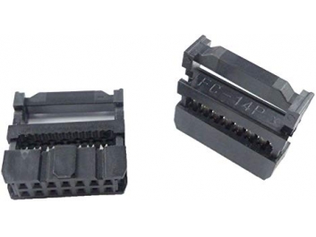
IDC CONNECTOR
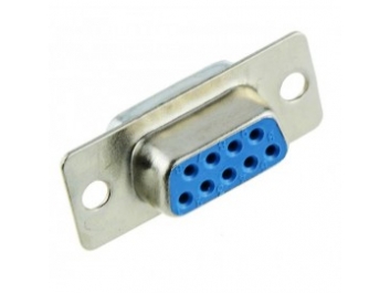
DB CONNECTOR
KF25 BLACK CONNECTOR
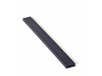
HEADER CONNECTOR
GREEN CONNECTOR
DC PIN JACK
HEAT SINK
HEAT SINK FOR TRANSISTOR
ICS
TTL AND CMOS IC
Microcontroller
Optocoupler
MIX IC
IC SOCKET
KEYPADS
KEYPAD MATRIX
LEDS
MIX LEDS
7 Segment Display
P10 LED MODULE
SMD LEDS
PROGRAMMER
IC PROGRAMMER
IC PROGRAMMER SOCKET
STM DISCOVERY BOARD
STM BOARD
TOOLS & DIGITAL MULTIMETER
DIGITAL MULTIMETER
TOOLS
VOLT METER AC DC
MECHANIC TOOLS
WIRE
JUMPER WIRE
CABLE WIRE
Transistor
Mosfet Transistor
Voltage Regulator
Smd Transistor
Mix Transistor
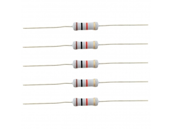
Resistor
Resistor Quarter Watt
Resistor Half Watt
Resistor 1 Watt
Resistor 2 Watt
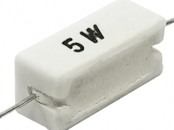
Resistor 5 Watt
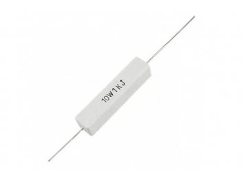
Resistor 10 Watt
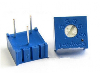
Variable Resistor
SMD Resistor
Capacitor Electronics
Ceramic Capacitor
Block Capacitor
Electrolytic Capacitor
SMD CAPACITOR
SWITCH
DIP SWITCH
PUSH SWITCH
RELAYS
BUZZER
POWER ADAPTER
POWER SUPPLY
PELTIER
PELTIER SET
FUSE
FUSE HOLDER
DIODE
sales@theicshop.org
0092 322 440 1074
Clear
Home
Shop
ARDUINO
Arduino & Development Board
Arduino SHIELDS
Arduino Modules
Arduino Relay Modules
Arduino LCDS
SERVO MOTOR
INCUBATOR CONTROLLER MODULE
Amplifier Module
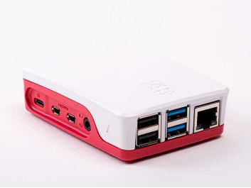
RASPBERRY PI
Raspberry PI LCDs
Raspberry PI BOARD
Raspberry PI MODULE
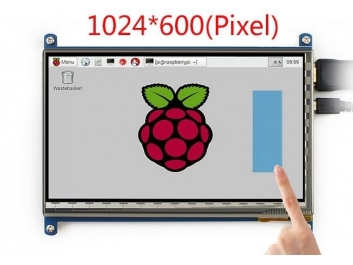
LCDS & DISPLAY
JHD LCD DISPLAY
Fuel Dispenser LCDS
Battery And Power Bank Kits
BATTERY
POWER BANK MODULE
Battery Management System
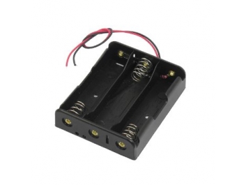
BATTERY HOLDER
Beard Board And Vero Board
Beard Board
Vero Board
Connector
IDC CONNECTOR
DB CONNECTOR
KF25 BLACK CONNECTOR
HEADER CONNECTOR
GREEN CONNECTOR
DC PIN JACK
HEAT SINK
HEAT SINK FOR TRANSISTOR
ICS
TTL AND CMOS IC
Microcontroller
Optocoupler
MIX IC
IC SOCKET
KEYPADS
KEYPAD MATRIX
LEDS
MIX LEDS
7 Segment Display
P10 LED MODULE
SMD LEDS
PROGRAMMER
IC PROGRAMMER
IC PROGRAMMER SOCKET
STM DISCOVERY BOARD
STM BOARD
TOOLS & DIGITAL MULTIMETER
DIGITAL MULTIMETER
TOOLS
VOLT METER AC DC
MECHANIC TOOLS
WIRE
JUMPER WIRE
CABLE WIRE
Transistor
Mosfet Transistor
Voltage Regulator
Smd Transistor
Mix Transistor
Resistor
Resistor Quarter Watt
Resistor Half Watt
Resistor 1 Watt
Resistor 2 Watt
Resistor 5 Watt
Resistor 10 Watt
Variable Resistor
SMD Resistor
Capacitor Electronics
Ceramic Capacitor
Block Capacitor
Electrolytic Capacitor
SMD CAPACITOR
SWITCH
DIP SWITCH
PUSH SWITCH
RELAYS
BUZZER
POWER ADAPTER
POWER SUPPLY
PELTIER
PELTIER SET
FUSE
FUSE HOLDER
DIODE
About Us
Contact Us
LOGIN
0
PKR 0
Cart is empty
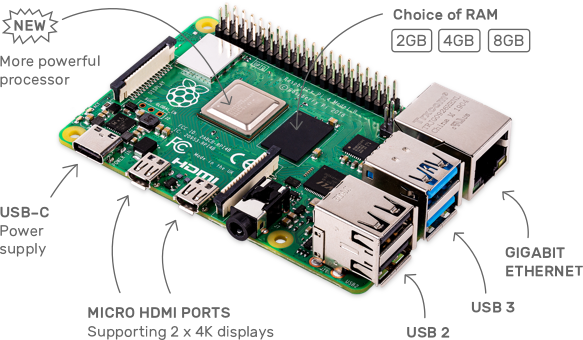
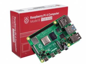
Raspberry Pi 4
Completely upgraded, re-engineered
Faster, more powerful
Starting From
PKR12000
Shop Now
ARDUINO
RASPBERRY PI
LCDS & DISPLAY
Battery And Power Bank Kits
Beard Board And Vero Board
Connector
HEAT SINK
ICS
KEYPADS
LEDS
PROGRAMMER
STM DISCOVERY BOARD
TOOLS & DIGITAL MULTIMETER
WIRE
Transistor
Resistor
Capacitor Electronics
SWITCH
POWER ADAPTER
PELTIER
FUSE
DIODE
Arduino & Development Board
View Products
Arduino SHIELDS
View Products
Arduino Modules
View Products
Arduino Relay Modules
View Products
Arduino LCDS
View Products
SERVO MOTOR
View Products
INCUBATOR CONTROLLER MODULE
View Products
Amplifier Module
View Products
All Categories
Raspberry PI LCDs
View Products
Raspberry PI BOARD
View Products
Raspberry PI MODULE
View Products
All Categories
JHD LCD DISPLAY
View Products
Fuel Dispenser LCDS
View Products
All Categories
BATTERY
View Products
POWER BANK MODULE
View Products
Battery Management System
View Products
BATTERY HOLDER
View Products
All Categories
Beard Board
View Products
Vero Board
View Products
All Categories
IDC CONNECTOR
View Products
DB CONNECTOR
View Products
KF25 BLACK CONNECTOR
View Products
HEADER CONNECTOR
View Products
GREEN CONNECTOR
View Products
DC PIN JACK
View Products
All Categories
HEAT SINK FOR TRANSISTOR
View Products
All Categories
TTL AND CMOS IC
View Products
Microcontroller
View Products
Optocoupler
View Products
MIX IC
View Products
IC SOCKET
View Products
All Categories
KEYPAD MATRIX
View Products
All Categories
MIX LEDS
View Products
7 Segment Display
View Products
P10 LED MODULE
View Products
SMD LEDS
View Products
All Categories
IC PROGRAMMER
View Products
IC PROGRAMMER SOCKET
View Products
All Categories
STM BOARD
View Products
All Categories
DIGITAL MULTIMETER
View Products
TOOLS
View Products
VOLT METER AC DC
View Products
MECHANIC TOOLS
View Products
All Categories
JUMPER WIRE
View Products
CABLE WIRE
View Products
All Categories
Mosfet Transistor
View Products
Voltage Regulator
View Products
Smd Transistor
View Products
Mix Transistor
View Products
All Categories
Resistor Quarter Watt
View Products
Resistor Half Watt
View Products
Resistor 1 Watt
View Products
Resistor 2 Watt
View Products
Resistor 5 Watt
View Products
Resistor 10 Watt
View Products
Variable Resistor
View Products
SMD Resistor
View Products
All Categories
Ceramic Capacitor
View Products
Block Capacitor
View Products
Electrolytic Capacitor
View Products
SMD CAPACITOR
View Products
All Categories
DIP SWITCH
View Products
PUSH SWITCH
View Products
RELAYS
View Products
BUZZER
View Products
All Categories
POWER SUPPLY
View Products
All Categories
PELTIER SET
View Products
All Categories
FUSE HOLDER
View Products
All Categories
All Categories
Featured Products
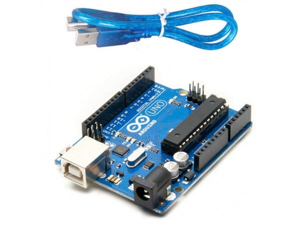
ARDUINO UNO R3 BOARD WITH CABLE
PKR 1500
Add to Cart
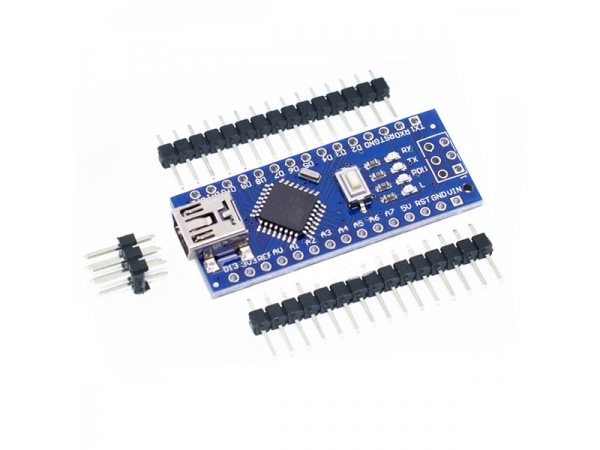
ARDUNO NANO WITHOUT CABLE
PKR 650
Add to Cart
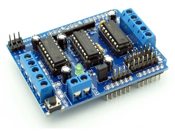
L293D SHIELD FOR ARDUINO UNO
PKR 400
Add to Cart
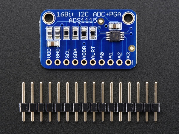
ADS1115 16 bits ADC precision analog-to-digital converter with 16-bits of resolution
PKR 1200
Add to Cart
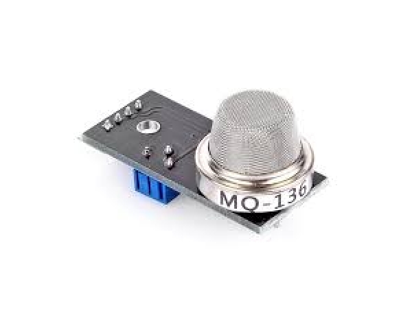
MQ136 Hydrogen Sulfide Detection Module
PKR 5000
Add to Cart
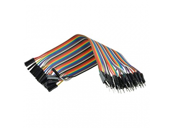
MALE TO FEMALE JUMPER WIRES DUPONT CABLES 20cm 8-INCH
PKR 150
Add to Cart
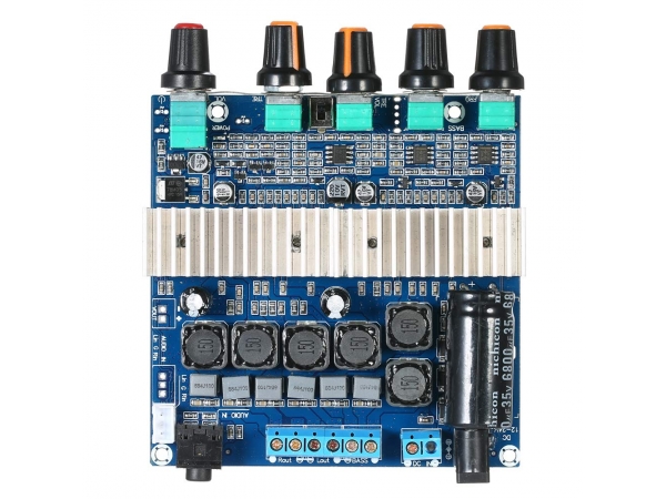
TPA3116 2.1 50W 50W 100W Amplifier Board
PKR 4000
Add to Cart
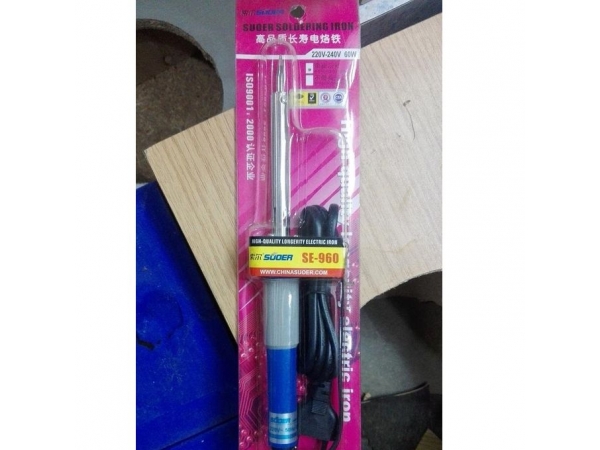
SOLDING IRON 60 WATT WITH LIGHT IN PAKISTAN
PKR 650
Add to Cart
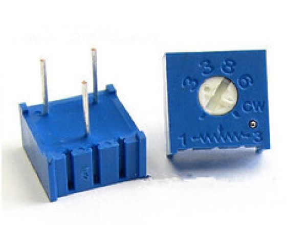
Trimpot 3386 Series Potentiometer
PKR 30
Add to Cart
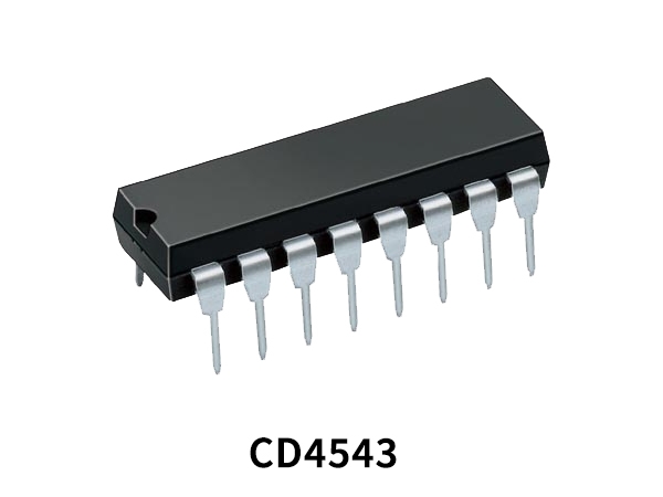
CD4543 IC Introduction to 7 Segment Display Chip
PKR 40
Add to Cart
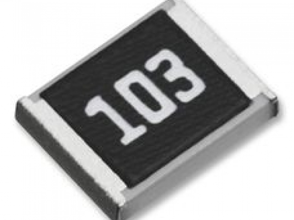
RESISTOR SMD 10R 1210 SIZE
PKR 10
Add to Cart
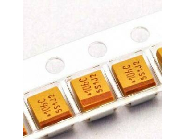
10UF 16V 1210 SIZE SMD CAPACITOR TANTALUM CAPACITOR
PKR 25
Add to Cart
New Arrival
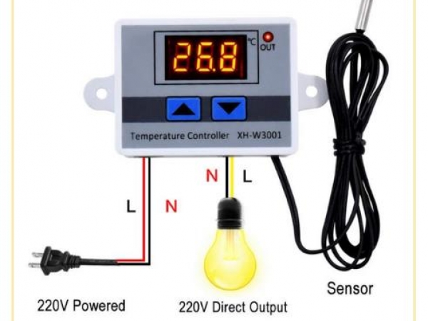
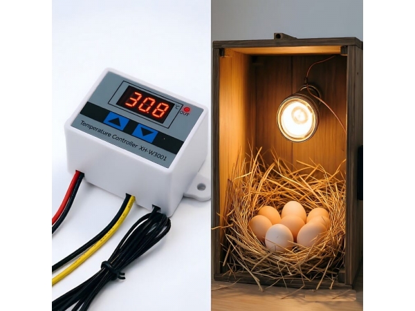
XH 3001 TEMPERATURE CONTROLLER AC 220V
PKR 500
Add to Cart
XH 3001 TEMPERATURE CONTROLLER 220V
PKR 500
Add to Cart
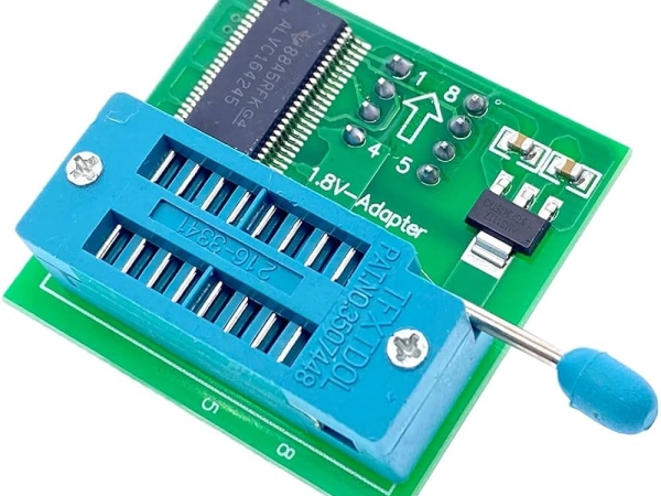
xcluma 1.8V Adapter For SPI Flash SOP8 DIP8 W25 MX25 for TL866CS TL866A EZP2010 EZP2013 EZP2019 CH341A
PKR 1000
Add to Cart
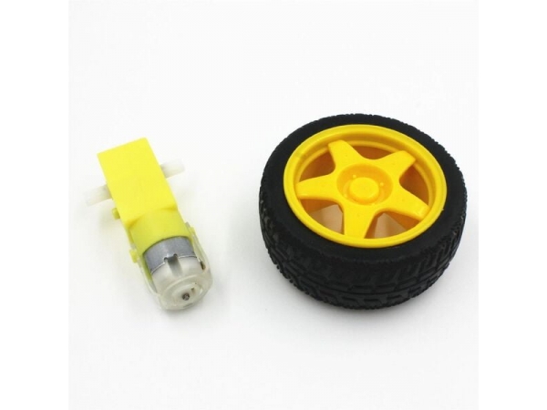
DC 3-6v TT Gear Motor And Rubber (Plastic) Wheel for Smart Car Robot
PKR 250
Add to Cart
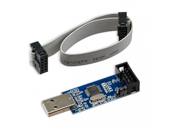
Programmer AVR Minimum System Board ATMEGA16 ATmega32 + USB ISP USBasp For ATMEL
PKR 600
Add to Cart
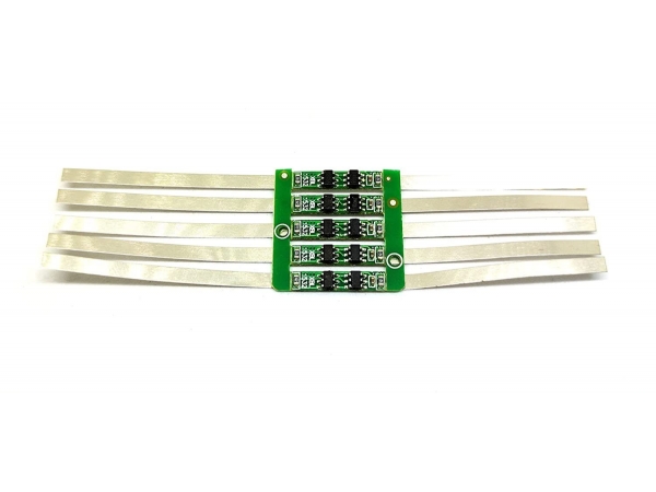
1S 18650 Lithium Battery Over Charge Protective Plat with Solder Belt Connector
PKR 35
Add to Cart
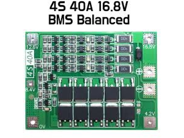
4s Bms 4s 40a Bms Li-ion Battery Protection Board Balanced Version In Pakistan 40 A BMS:
PKR 350
Add to Cart
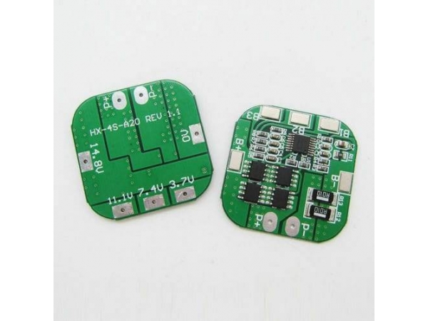
4S 20A 14.8v Bms For 18650 Lithium Ion Cells Battery Protection Board
PKR 250
Add to Cart
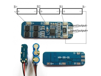
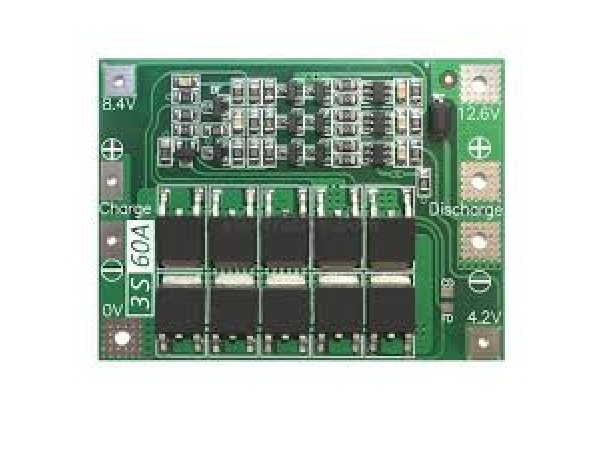
3S 25A BMS Circuit In Pakistan Li-ion Battery Charging Protection In Pakistan
PKR 300
Add to Cart
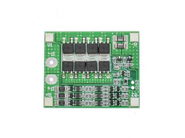
3S 60A 18650 Lithium Battery Protection Board With Equalization
PKR 350
Add to Cart
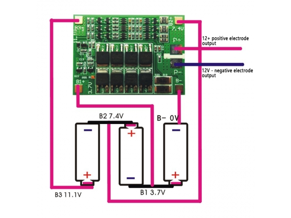
3s 40a Bms 11.1v 12.6v 18650 Lithium Battery Protection Board With 100ma Balancing Feature
PKR 300
Add to Cart
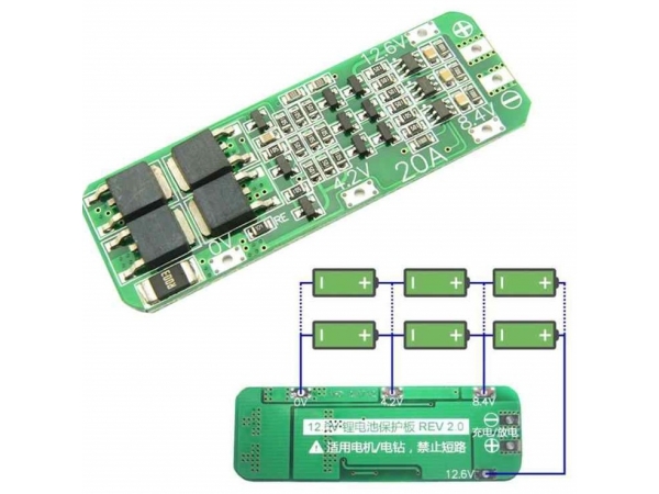
3S 20A BMS Module For Lithium Batteries
PKR 200
Add to Cart
Add to cart
×
Please wait...